
From Gnd To Functionality: How Pcba Suppliers Ensure Signal Integrity
When designing or assembling a printed circuit board (PCB), one of the most overlooked yet critical elements is signal integrity — the ability of a signal to propagate through a circuit without being distorted, delayed, or lost. And it all starts with one essential concept: GND (Ground).
As experienced PCBA suppliers, we understand that a functional board isn’t just about placing components correctly — it’s about ensuring clean, stable, and interference-free signal transmission. In this article, we’ll walk you through how PCBA professionals approach grounding and signal integrity to deliver high-performance electronics.
What Is Signal Integrity and Why Does It Matter?
Signal integrity (SI) refers to the quality and reliability of an electrical signal as it travels through a PCB. Poor signal integrity can result in:
- Crosstalk between traces
- Voltage reflections
- Ground bounce
- Electromagnetic interference (EMI)
- Data loss or functional failures
For high-speed or sensitive applications, such as medical devices, aerospace electronics, and communication equipment, signal integrity can be the difference between success and failure.
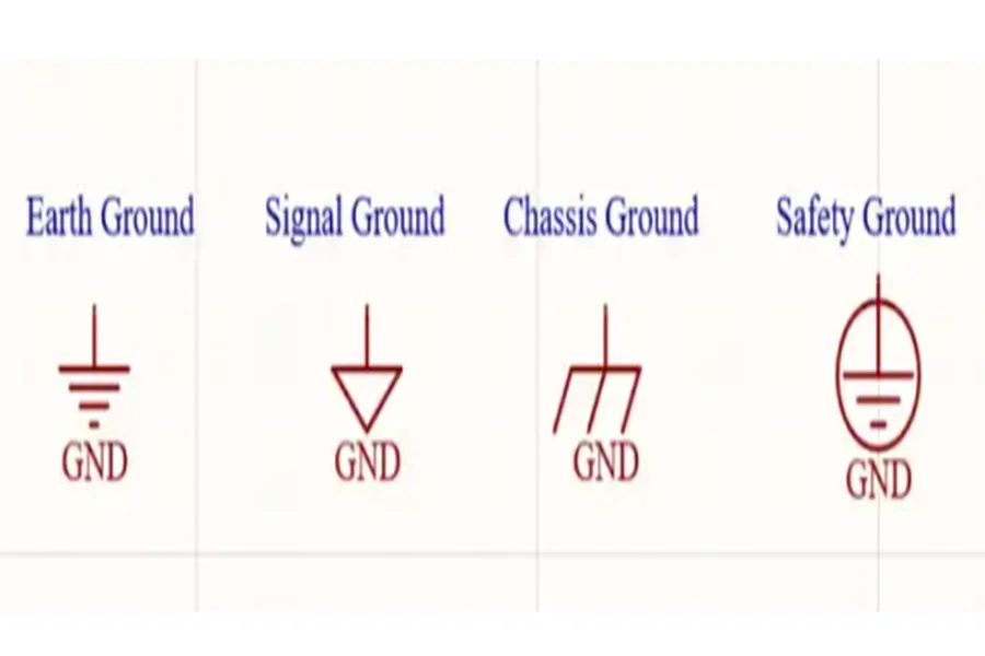
Why GND Is the Foundation of Signal Integrity
In every PCB, GND (ground) is more than just a return path for current — it’s the reference voltage for all signals and the anchor point for stability.
A well-designed ground system:
- Provides a low-impedance return path
- Minimizes ground loops and noise
- Reduces EMI and RF emissions
- Enhances power distribution and thermal management
PCBA suppliers play a key role in ensuring that GND planes and vias are optimally placed for both performance and manufacturability.
How PCBA Suppliers Ensure Ground Integrity and Signal Quality
Here’s how experienced PCBA manufacturers like PCBasic maintain signal integrity, starting from GND and extending throughout the entire board:
-
Dedicated GND Planes
A continuous, unbroken ground plane in multilayer PCBs provides a stable return path for high-speed signals. We ensure:
- No interruptions by traces or vias
- The separation between analog and digital grounds
- Consistent layer stack-ups
This reduces inductive coupling and enhances high-frequency performance.
-
Strategic Placement of Ground Vias
Poor via placement can break return paths and cause loop area expansion, leading to increased EMI. We:
- Add sufficient ground stitching vias near signal layer transitions
- Use via-in-pad technology when needed
- Minimize ground return paths for sensitive signals
-
Controlled Impedance Routing
For differential pairs (e.g., USB, HDMI, Ethernet), PCBA suppliers must maintain consistent trace width, spacing, and dielectric thickness. Impedance mismatches lead to signal reflection and degradation.
We use PCB simulation tools and controlled impedance fabrication to meet these specs.
-
Shielding and Filtering Components
We design and place shielding cans, ferrite beads, and bypass capacitors near power and GND pins to suppress noise. Proper component selection and placement is essential to eliminate high-frequency interference.
-
DFM + SI Collaboration
We combine Design for Manufacturability (DFM) and Signal Integrity (SI) practices. Our engineering team works with clients to:
- Review ground/power plane separation
- Analyze the return current paths
- Suggest layout improvements for the clock and high-speed lines
This proactive support reduces costly revisions and ensures first-pass success.
Real-World Impact: What Clients Gain
By working with a professional PCBA supplier who understands grounding and SI:
- Products have fewer EMC issues
- Data transfer remains reliable at high speeds
- Circuit boards perform consistently in mission-critical environments
- You avoid delays from failed compliance testing or board redesigns
Conclusion: Ground First, Functionality Follows
Signal integrity isn’t something you “check later” — it starts with ground design. A clean, continuous GND layout is the backbone of any well-functioning PCB, especially in high-reliability applications.
At PCBasic, we help customers achieve signal integrity not just by assembling boards, but by building intelligence, engineering insight, and precision into every step of the process.